Scanning Electron Microscopy (SEM) and Energy Dispersive X-ray Spectroscopy (EDS)
Two powerful techniques commonly for imaging and elemental analysis of samples at a microscopic or even nanoscopic scale. SEM is a microscopy technique that uses a focused beam of electrons to scan the surface of a sample, generating high-resolution images that reveal the sample's topography and morphology. SEM images provide detailed information about the surface structure, texture, and morphology of the sample, with magnification ranging from around 10x to over 100,000x.
SEM can reveal features at nanometer scales and is especially useful for examining the microstructure of materials, studying biological samples, and analysing particle morphology. EDS is an analytical technique that is often integrated with SEM to provide elemental composition information about the sample's surface. It works by detecting X-rays emitted when electrons from the SEM beam interact with the sample's atoms. EDS provides qualitative and quantitative elemental analysis of the sample, allowing researchers to determine the presence and relative abundance of different elements. This information can be superimposed onto SEM images to create elemental maps, which show the spatial distribution of elements within the sample.
Combining SEM and EDS allows researchers to gain comprehensive information about a sample's morphology, structure, and elemental composition, making these techniques invaluable tools in various scientific and industrial applications, such as materials characterisation, failure analysis, and quality control.
Equipment
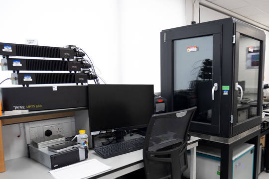
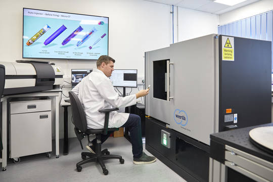
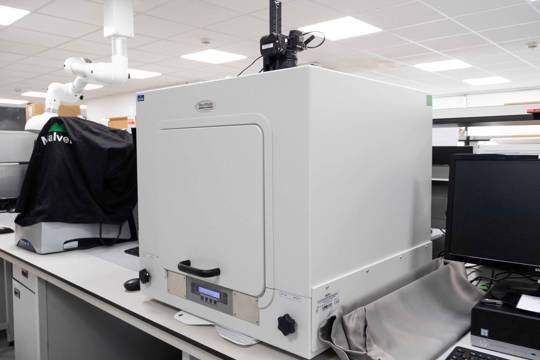
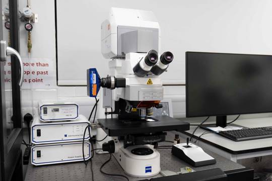
- JEOL JSM-6480-LV Low Vacuum Scanning Electron Microscope with Oxford Instruments X-Max 80 mm2 energy dispersive SDD X-ray detector and AZtecPharma software.
- JEOL JSM-IT500 - Low Vacuum Scanning Electron Microscope with Oxford Instruments X-Max 150 mm2 energy dispersive SDD X-ray detector and AZtecPharma software; Deben Peltier Stage (-25°C - 160°C).
